BASE
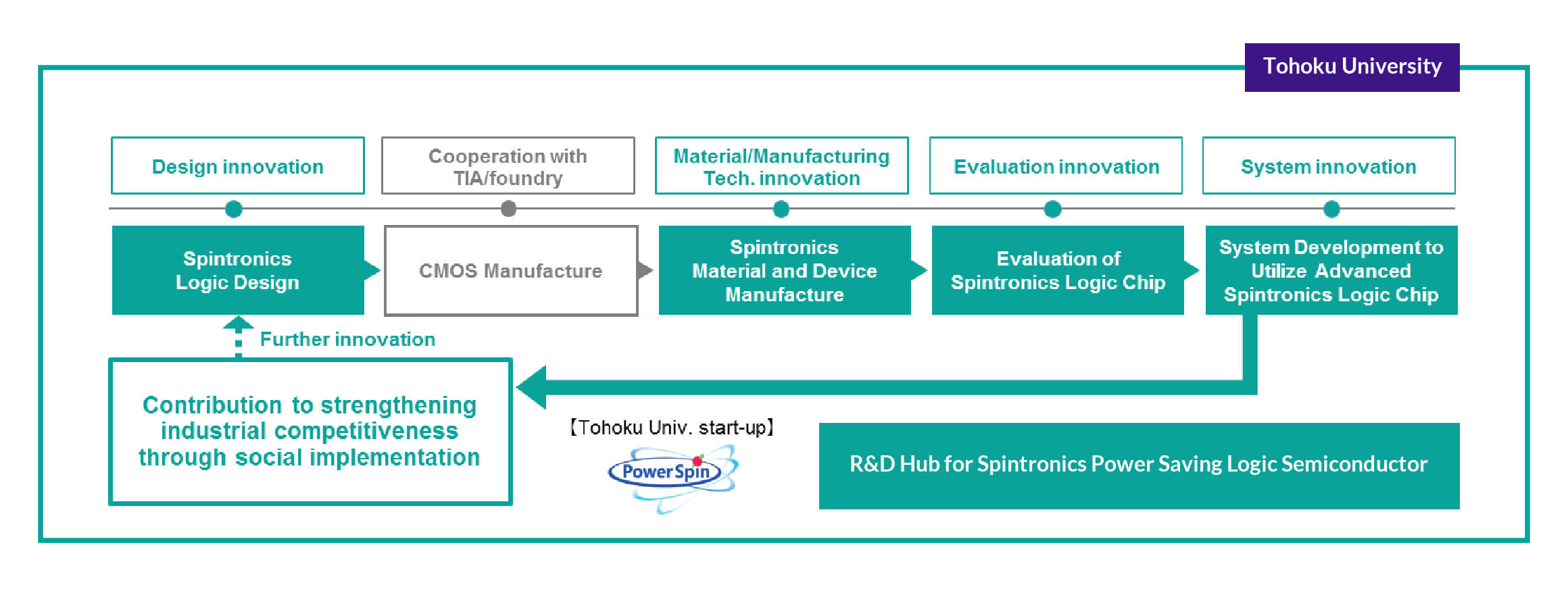
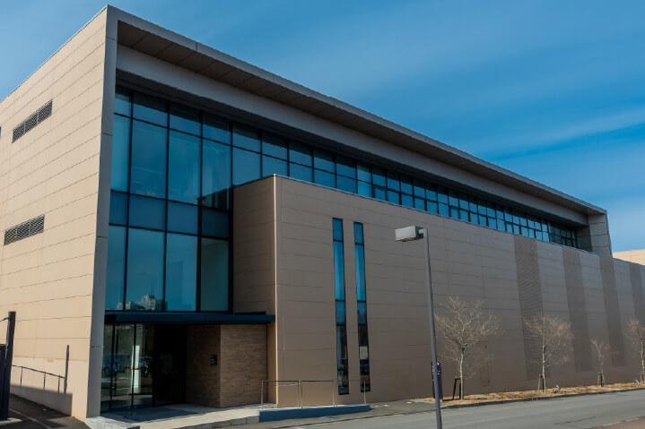
Spintronics Low-Power Semiconductor Development Hub
Leading the World in the Development of Spintronics Semiconductors and Their Application Systems
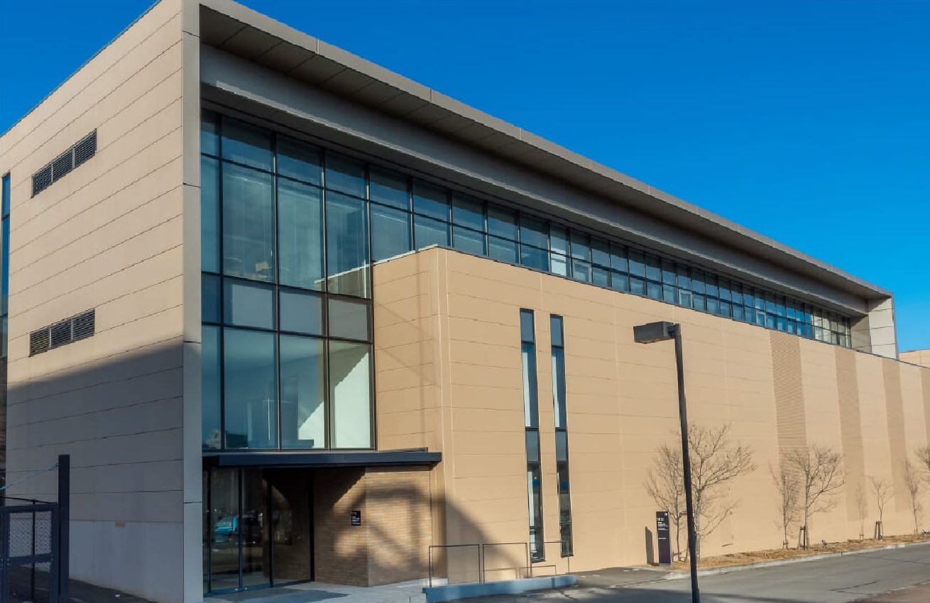
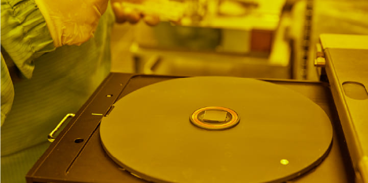
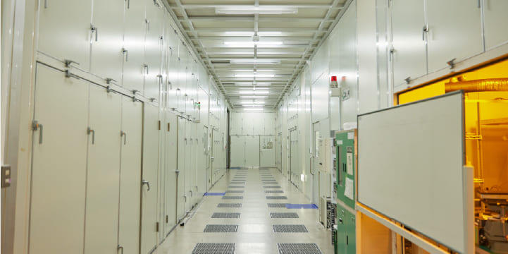
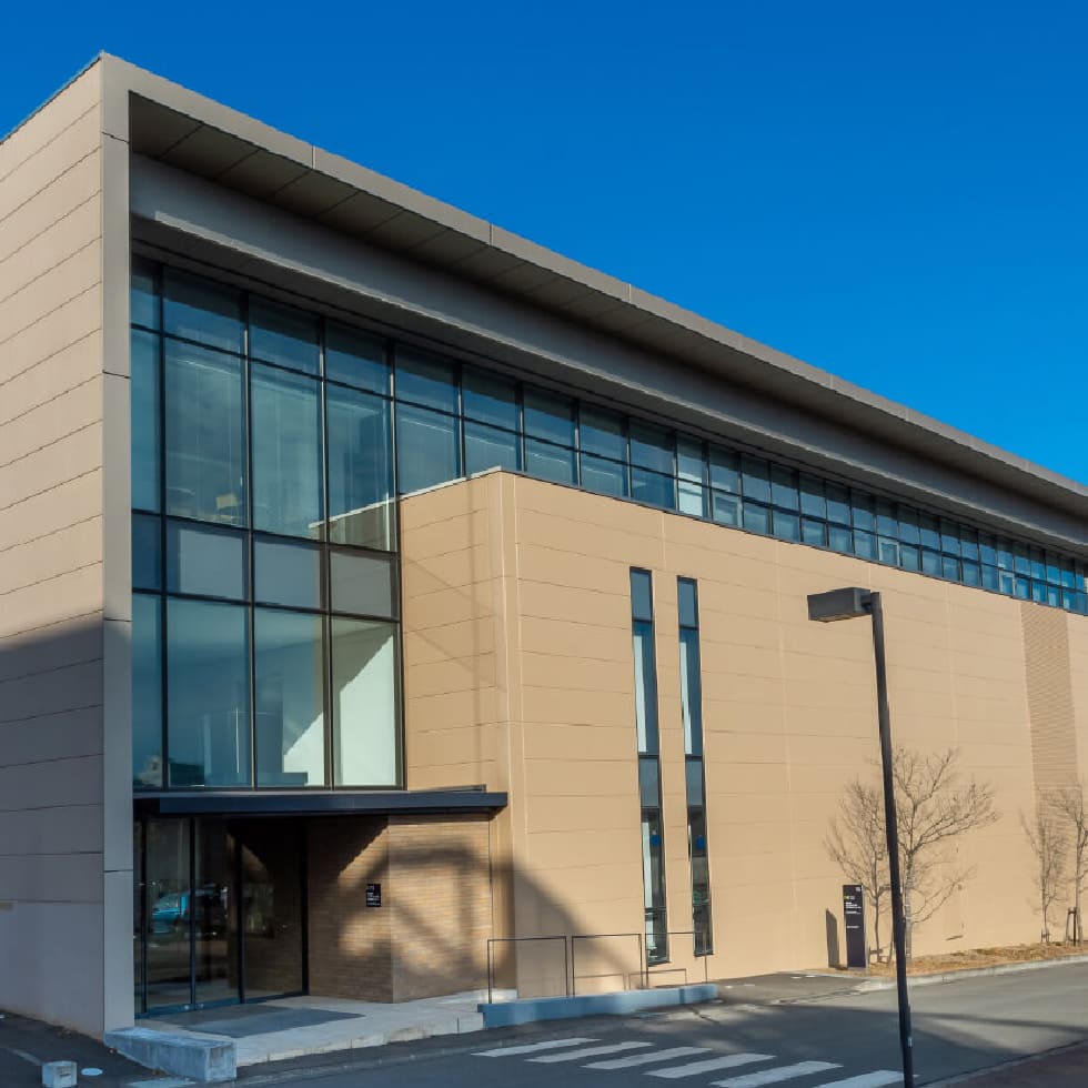
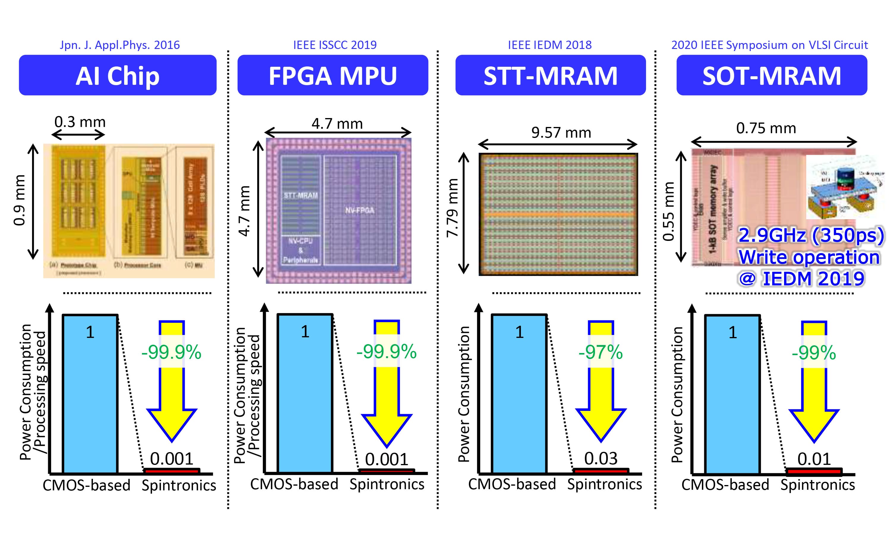
This center is the world's only R&D facility compatible with 300mm wafer processes in spintronics low power semiconductor development. We enable integrated development from design, material, device, chip demonstration, and system integration. Through this, we lead the world in developing spintronics logic semiconductors—a world-leading low power technology that reduces power consumption to 1/100—and their applied systems.
Awards
-
14th Prime Minister’s Awards for its Contribution to Industry-Academia-Government Collaboration (Professor Tetsuo Endoh)
-
2017 National Invention Award (Professor Tetsuo Endoh)
Strengths
-
01
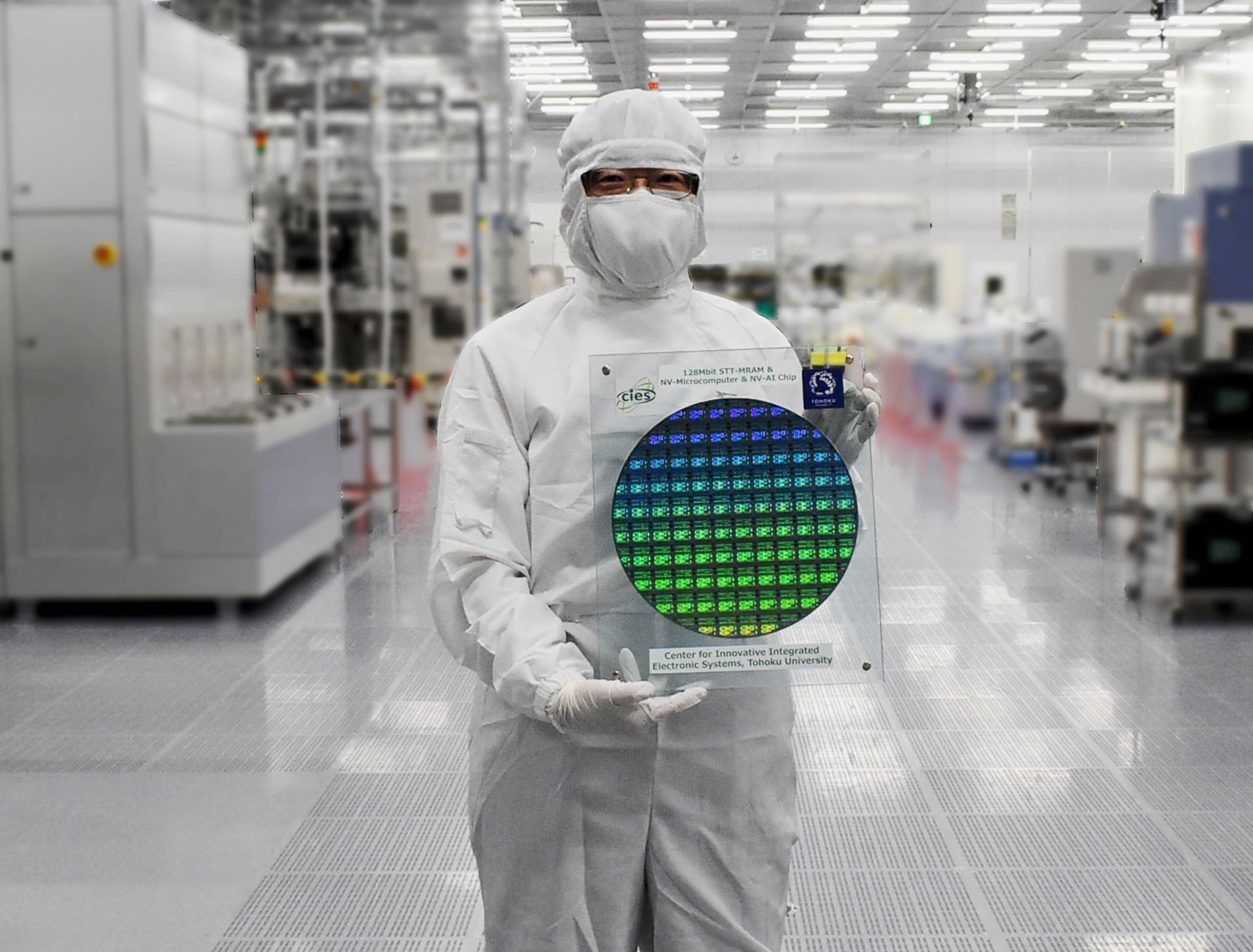
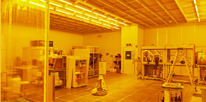
1,900㎡ CR & 300mm-Wafer line
-
02
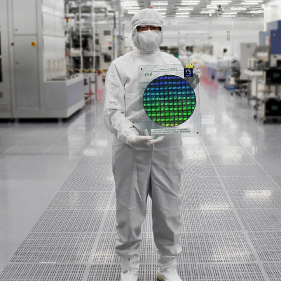
The world's only 300mm process-compatible prototyping line
-
03
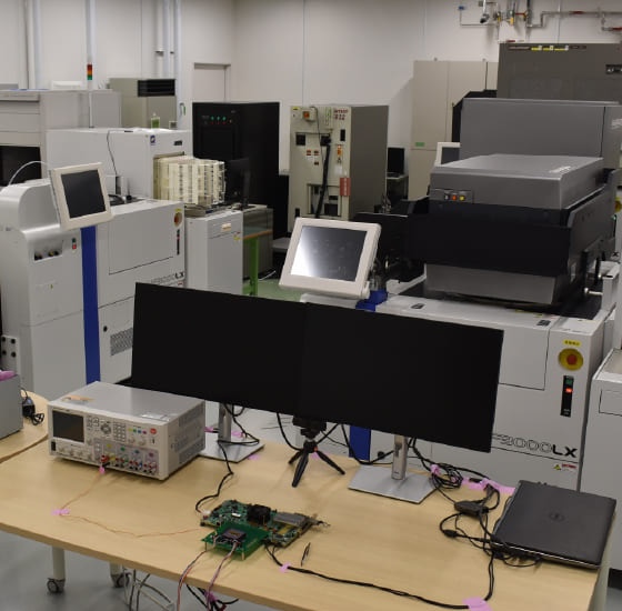
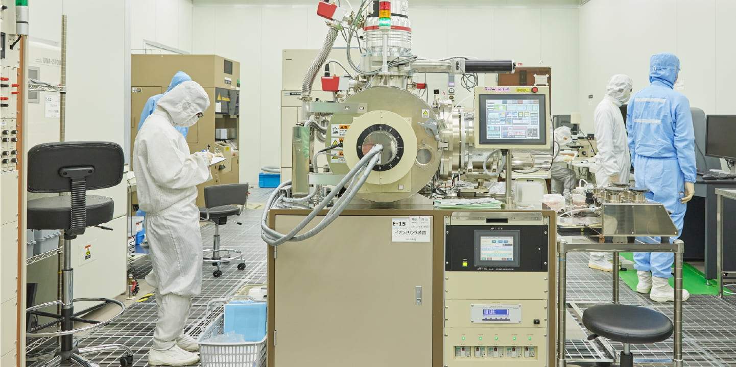
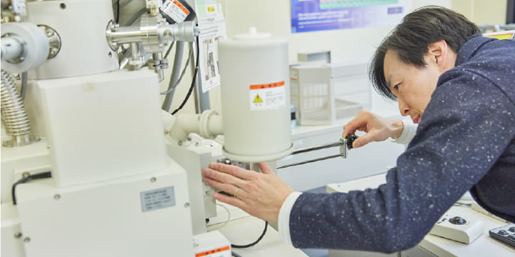
A comprehensive range of evaluation and analysis equipment for chip demonstration and testing
Capable of integrated development and demonstration from design, material, device, chip demonstration, and system integration
Case Studies
Researchers
-
Professor
Tetsuo Endoh
Toward the realization of a future carbon-neutral society, I am conducting research on (1) green electronics technology (low-power technology) to reduce the operating power of semiconductor chips—ranging from memory to AI, IoT, FPGA, and GPU processors that process information in various systems— and (2) power electronics technology (high-efficiency power conversion technology) to achieve highly efficient power management. Simultaneously, I am promoting industrial-academic collaborative development for practical application. Furthermore, I am committed to contributing to the development of human resources, including young researchers and engineers.
-
Professor
Yoshikazu Takahashi
I am developing power modules, power units, and their applied products—such as next-generation inverters and converters—that maximize the superior low-loss and high-frequency characteristics of SiC power devices and lateral GaN on Si power devices.
BASE
-
Spintronics Low-Power Semiconductor Development Hub
Design, Prototype verification, Evaluation and System development for
・Power saving logic semiconductor,
・AI processor,
・Next generation embedded memory (MRAM) with spintronics technology.VIEW DETAIL
-
Hub for Semiconductor Manufacturing Process, Parts, Material and Image Sensors
R&D based on ultra-clean process technology and image sensor technology for
・Ultra-small particles during manufacturing,
・Visualize gas flows,
・Ultra-clean parts,
・High-performance image sensor, Wiring materialsVIEW DETAIL
-
MEMS Design/Process Development Demonstration Hub
R&D and technological evaluation/phototyping for advanced mounting technology for devices such as
・inertial sensor,
・photonics,
・Communication,
etc. for autonomous vehicles.VIEW DETAIL
-
Smart System Ultra-Integration Research and Development Center
This organization was reorganized and renamed in April 2026 to promote research into next-generation smart systems, including chiplet integration, 3D packaging, silicon photonics, quantum and biosensors, and the integration of edge AI.
VIEW DETAIL