BASE
MEMS Design/Process Development Demonstration Hub
"Prototyping Coin Laundry"
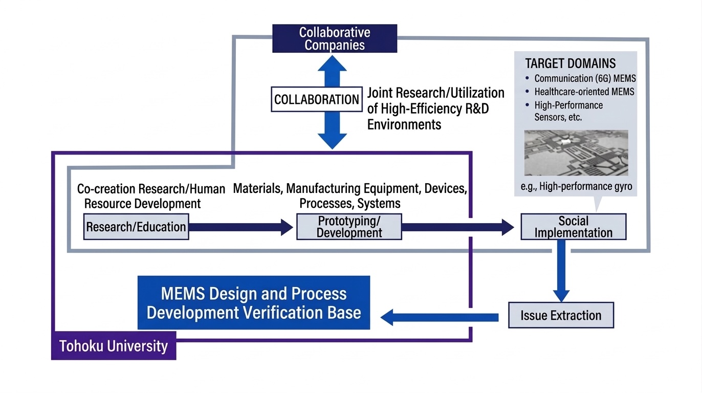
Where Open Collaboration Accelerates
R&D and Human Resource Development
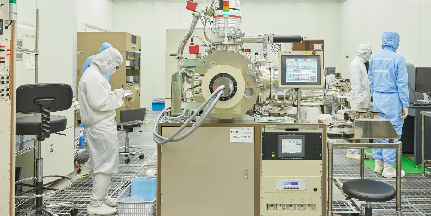
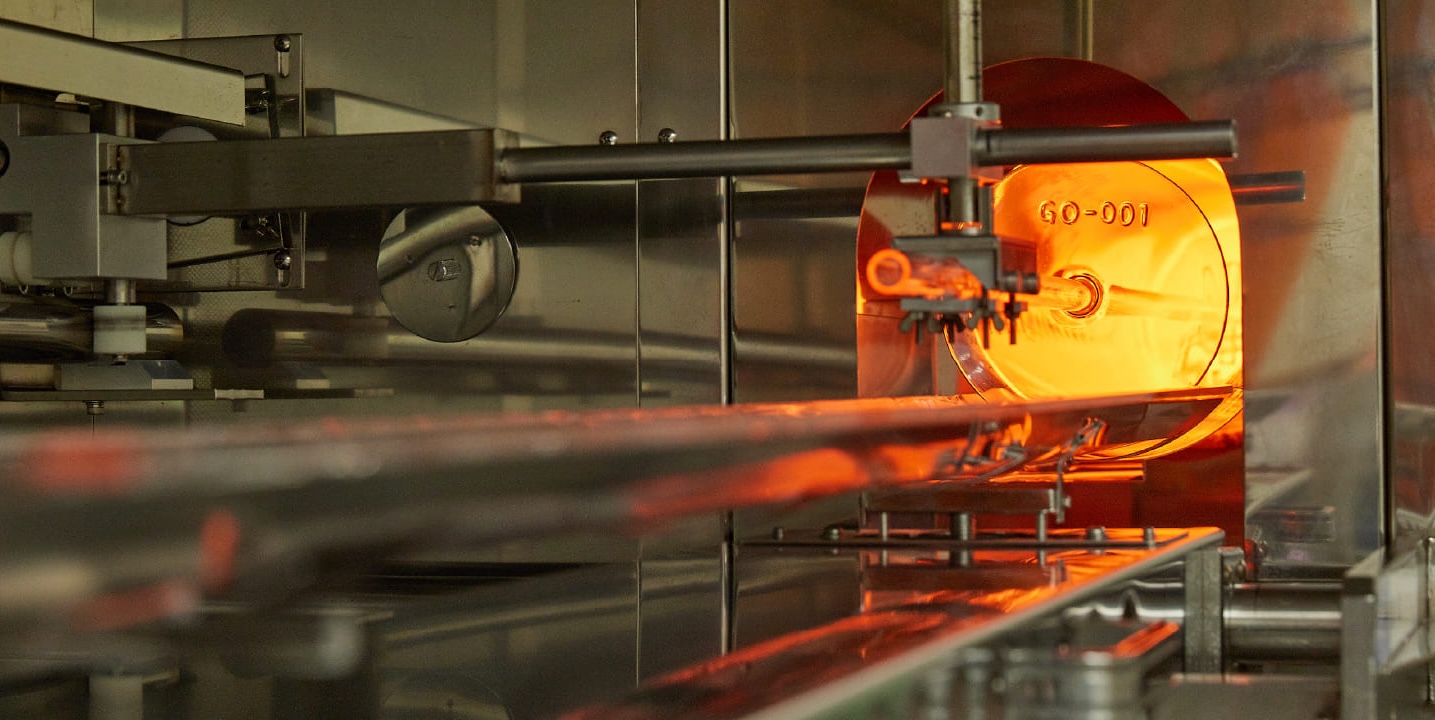
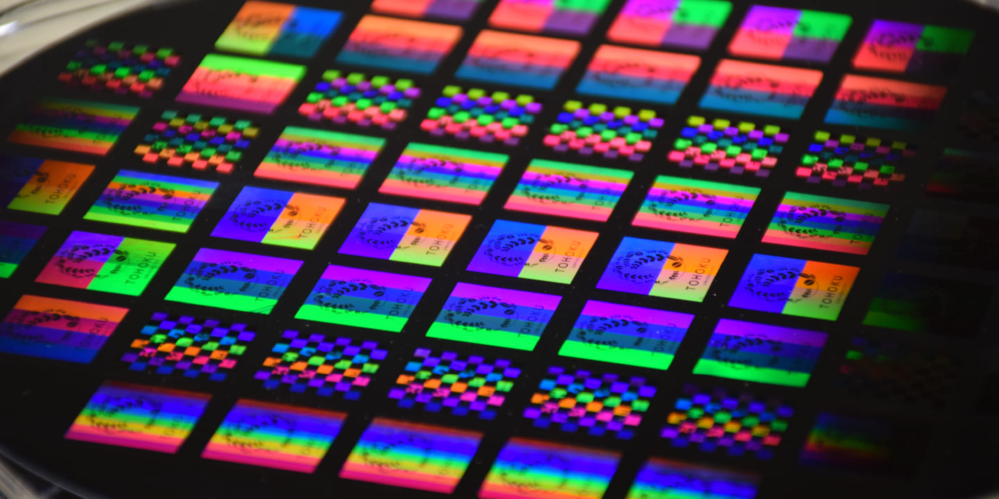
As one of the world's leading and Japan's largest R&D centers in the MEMS field, this facility promotes an integrated process from research to social implementation, including material/process development, design, prototyping, and evaluation. Our open prototyping line supports everything from small chips to 200mm wafers, enabling versatile research and development for MEMS, high-frequency devices, optical devices, and more. With support from our highly experienced staff, users can gain hands-on experience in every stage of the process, fostering human resource development alongside technological innovation.
Awards
-
4th Nanotechnology Platform Award for Outstanding Contribution (2017)
-
2nd Nanotechnology Platform Award for Contribution (2015)
-
2013 Ministry of Economy, Trade and Industry (METI) Award for Academic-Industrial Collaboration Merit
Strengths
-
01
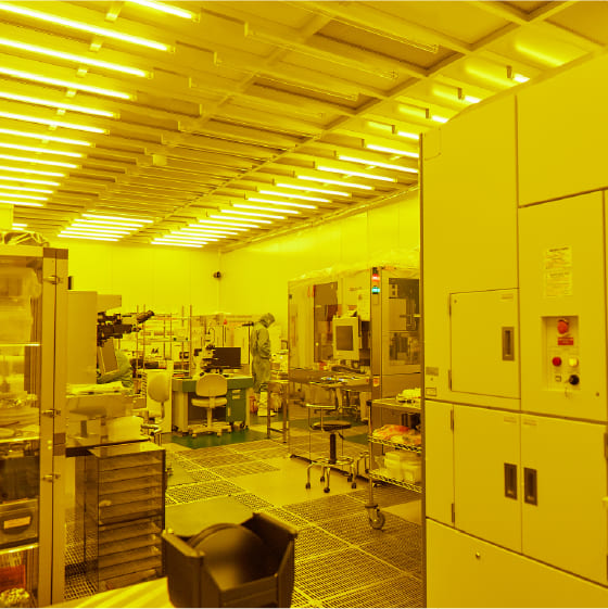
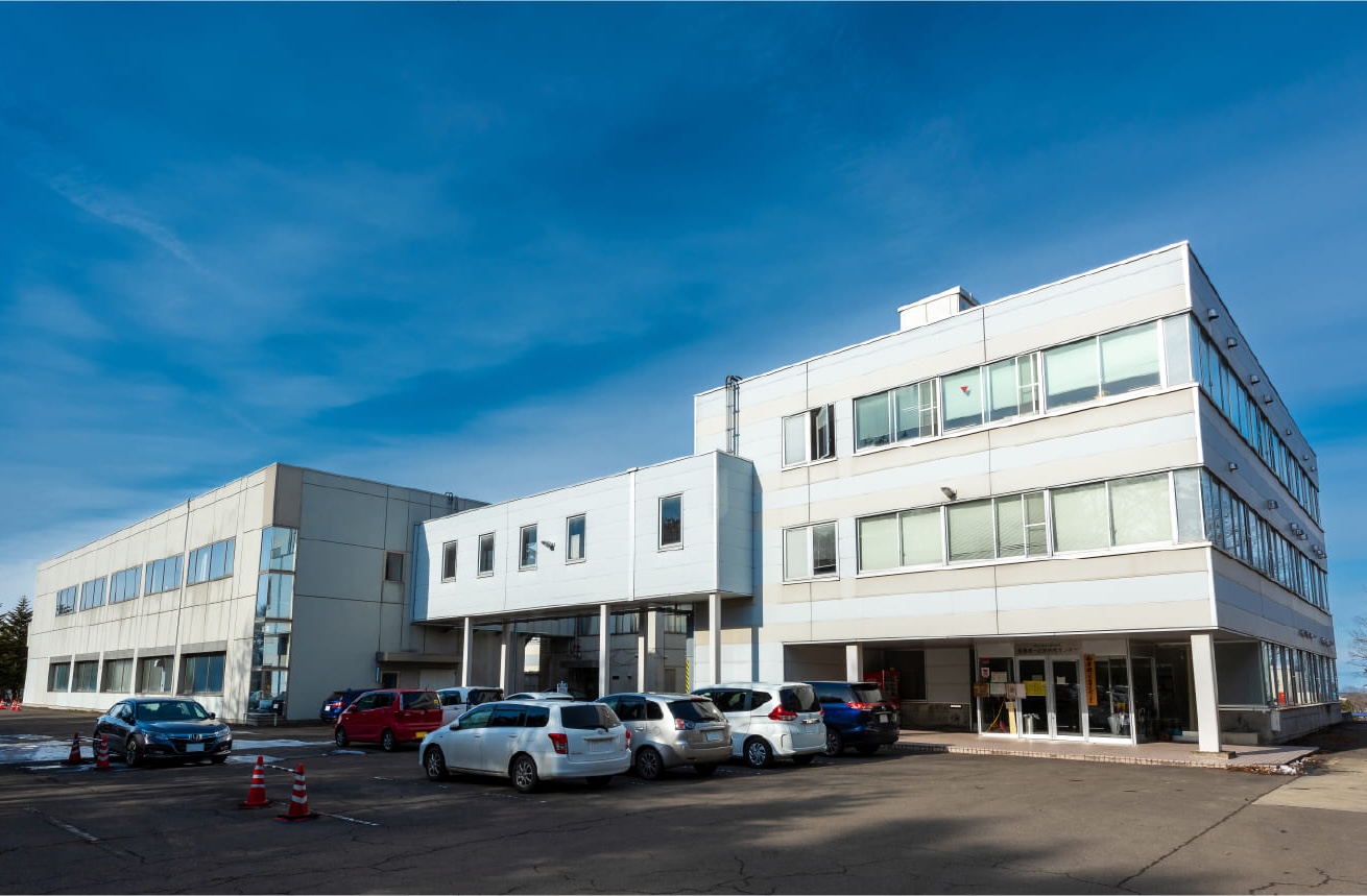
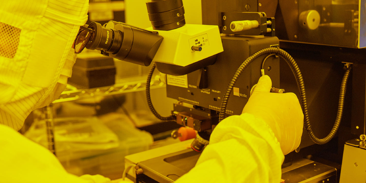
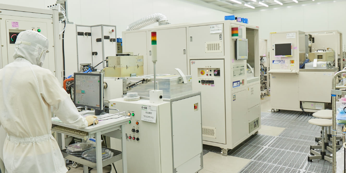
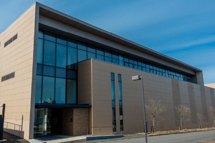
Utilizing the building that formerly housed the Semiconductor Research Institute—where Dr. Jun-ichi Nishizawa, known as "Mr. Semiconductor," served as Honorary Director—the facility boasts a 1,800㎡ cleanroom equipped with over 150 units of semiconductor manufacturing equipment, primarily for MEMS.
-
02
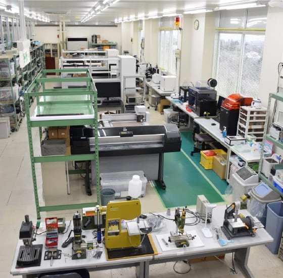
We also support electronic work and machining, providing an environment for the seamless prototyping, evaluation, and packaging of semiconductor devices. We actively support commercialization through collaboration with private enterprises.
-
03
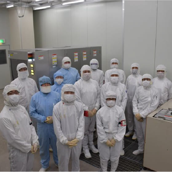
We provide technical support backed by accumulated know-how and a highly experienced professional staff.

BASE
-
Spintronics Low-Power Semiconductor Development Hub
Design, Prototype verification, Evaluation and System development for
・Power saving logic semiconductor,
・AI processor,
・Next generation embedded memory (MRAM) with spintronics technology.VIEW DETAIL
-
Hub for Semiconductor Manufacturing Process, Parts, Material and Image Sensors
R&D based on ultra-clean process technology and image sensor technology for
・Ultra-small particles during manufacturing,
・Visualize gas flows,
・Ultra-clean parts,
・High-performance image sensor, Wiring materialsVIEW DETAIL
-
MEMS Design/Process Development Demonstration Hub
R&D and technological evaluation/phototyping for advanced mounting technology for devices such as
・inertial sensor,
・photonics,
・Communication,
etc. for autonomous vehicles.VIEW DETAIL
-
Smart System Ultra-Integration Research and Development Center
This organization was reorganized and renamed in April 2026 to promote research into next-generation smart systems, including chiplet integration, 3D packaging, silicon photonics, quantum and biosensors, and the integration of edge AI.
VIEW DETAIL