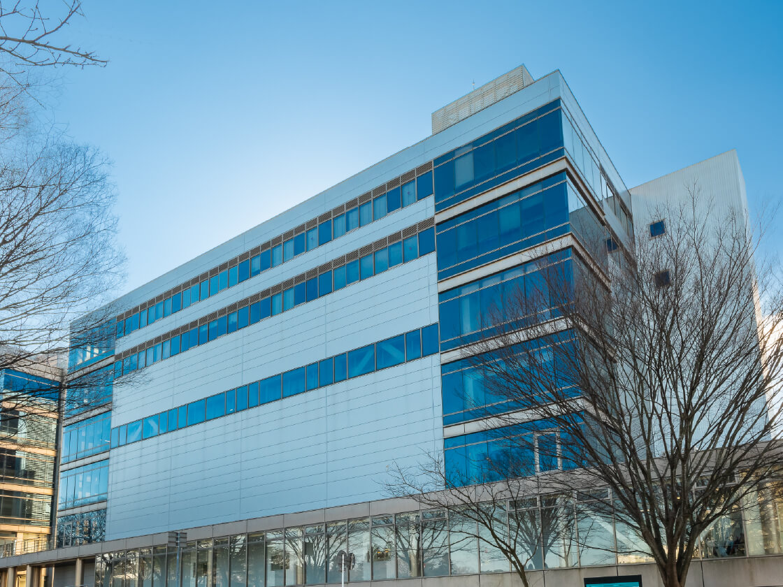
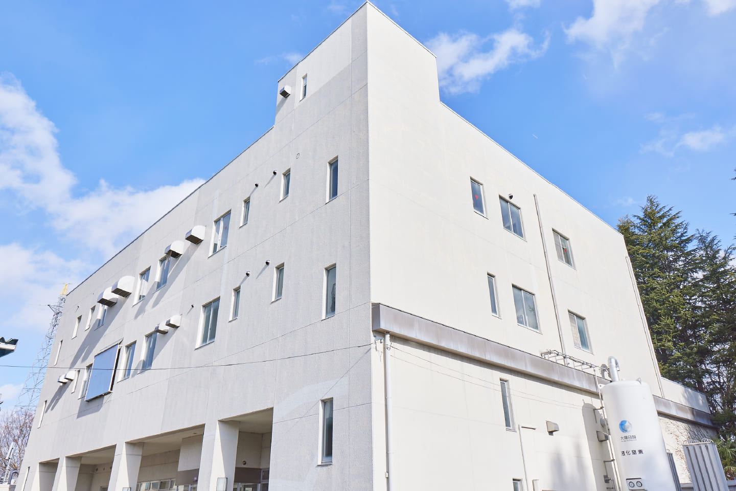
BASE
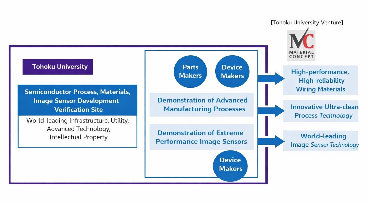
Hub for Semiconductor Manufacturing Process, Parts, Material and Image Sensors
Device Prototyping, Process & Material Development / Evaluation / Testing
~Capable of meeting diverse research and development needs, from trial experiment levels to prototype evaluation levels~
This center boasts world-class infrastructure and utilities, and by sharing them, it provides a challenging open innovation platform that comprehensively and simultaneously promotes research and development on cutting-edge devices, materials, equipment, and components through industry-academia collaboration, leading to practical application and social implementation.
Strengths
-
01
-
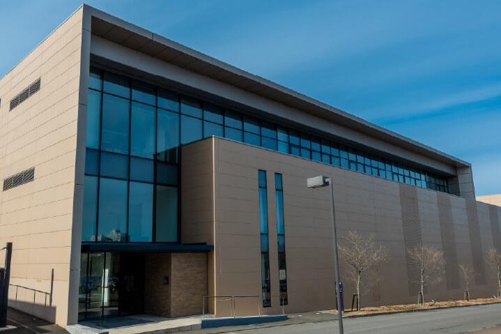
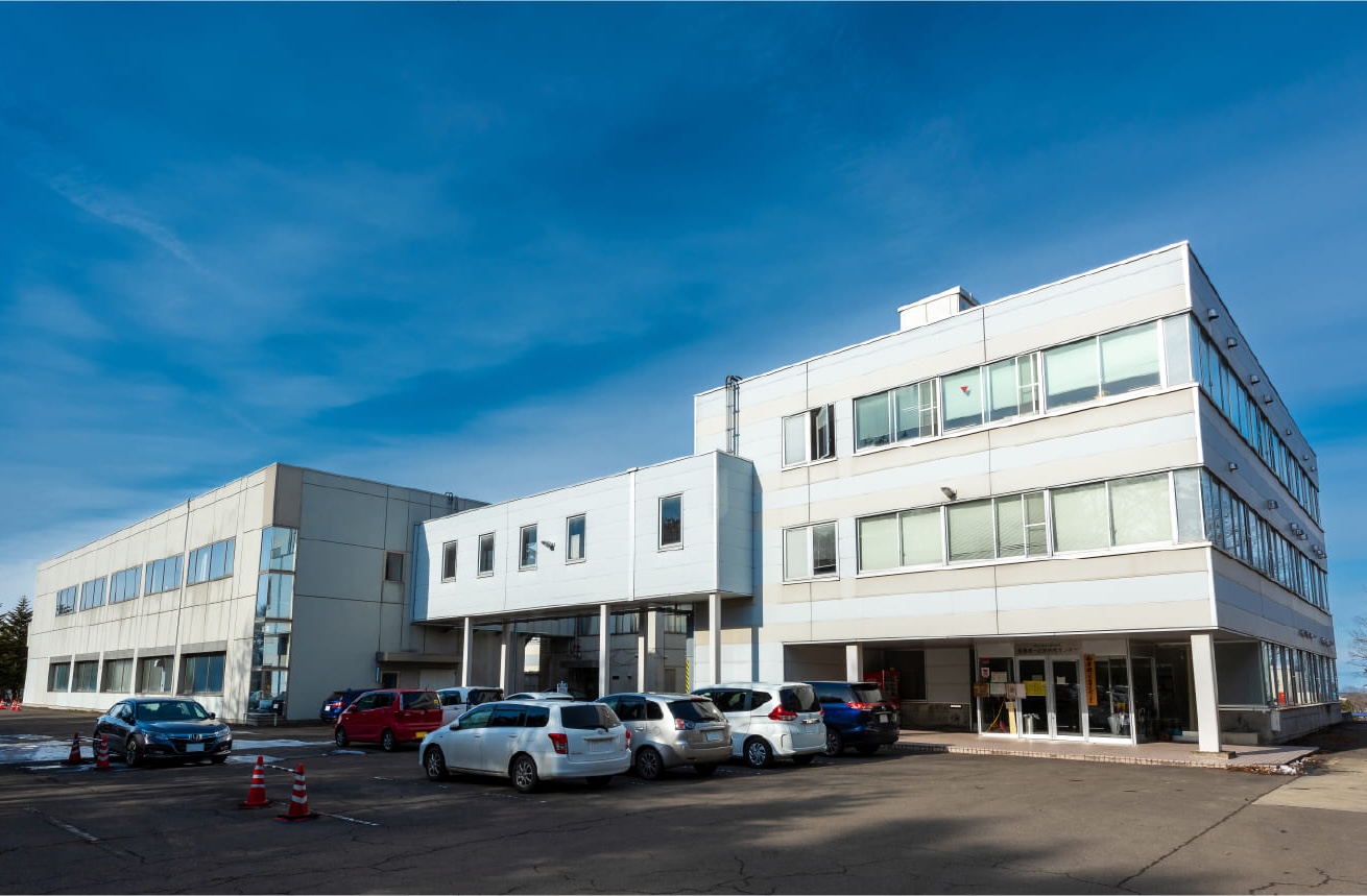
02
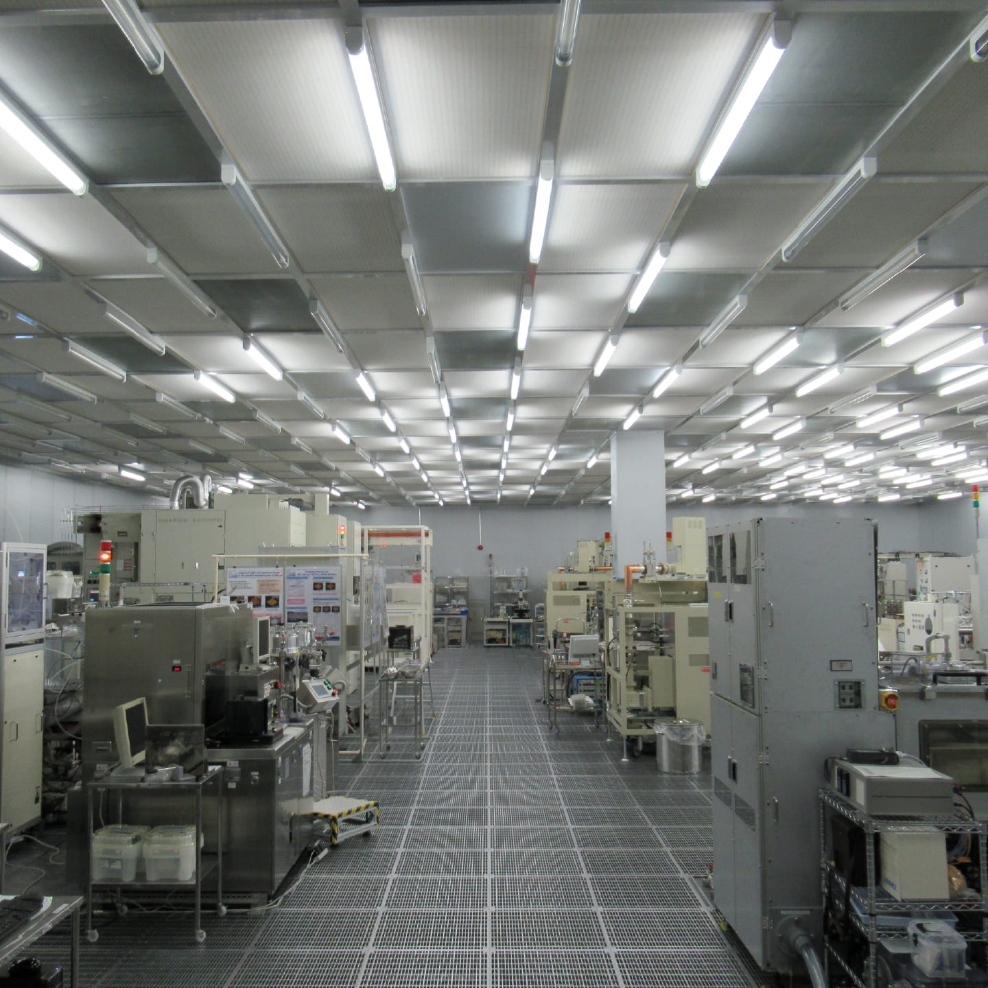
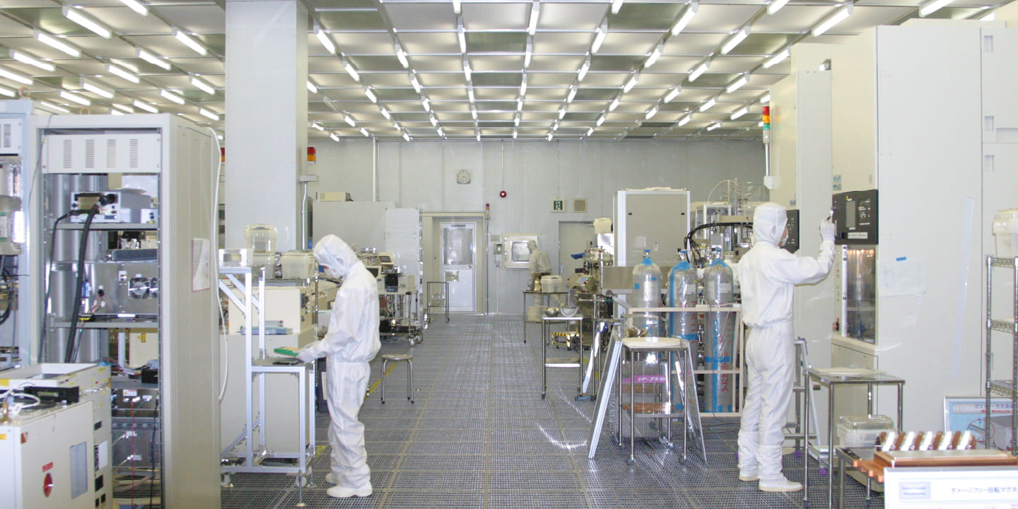
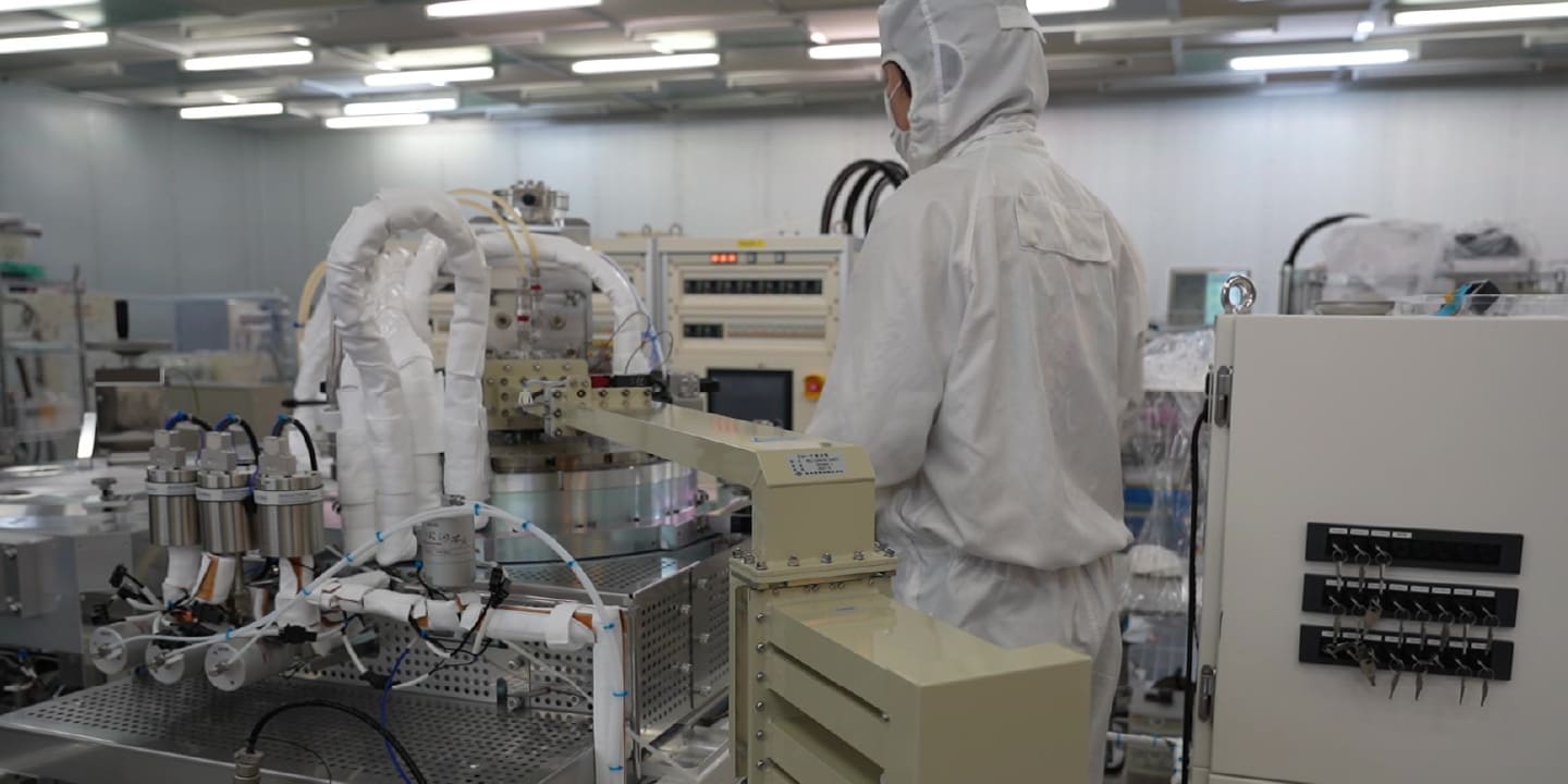
Experimental equipment in the cleanroom on the 4th floor of the Fluctuation-Free Facility for New Information Industry
-
03
Researchers
-
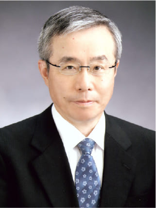
Professor
Rihito Kuroda
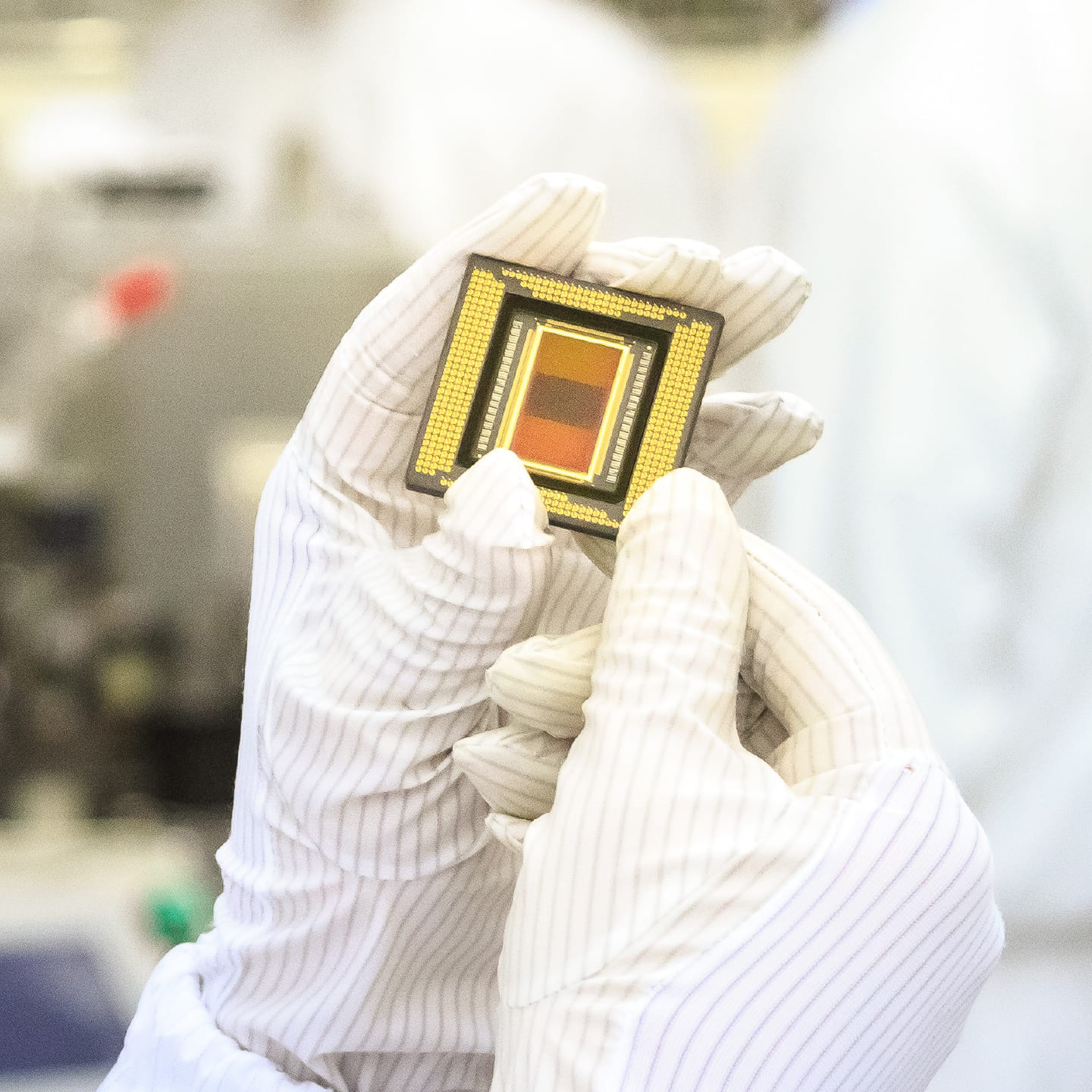
I am promoting the development and commercialization of high-performance semiconductor devices and image sensors featuring high sensitivity, wide dynamic range, high speed, wide optical wavelength bands, and high reliability that surpass the capabilities of the human eye. We are also advancing advanced sensing applications for semiconductor manufacturing processes and the practical application of the world's highest-performance soft X-ray detectors used at the Tohoku Synchrotron Radiation Facility.
-
Professor
Yasuyuki Shirai
We are deepening and evolving the development of materials and components for advanced semiconductor-grade ultra-clean equipment, as well as outgassing and particle contamination measurement and evaluation technologies—fields in which Tohoku University has long led the world. These infrastructure technologies serve not only as the foundation for the advanced semiconductor sector but are also being expanded into other manufacturing industries. Additionally, we provide cleanroom facilities and equipment as a venue for open innovation.
-
Professor
Shigetoshi Sugawa
Utilizing the NICHe (New Industry Creation Hatchery Center) the Fluctuation-Free Facility for New Information Industry, which houses world-class advanced cleanroom facilities, I am promoting industrial-academic collaborative development. Our goal is to further strengthen the competitiveness of Japan's strengths—silicon semiconductor materials, manufacturing equipment technology, and image sensor/device technology—while pioneering new technological fields.
-
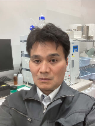
Specially Appointed Professor
Masayoshi Takahashi
While exploring the mechanisms of micro/nanobubble water, I am developing applications for semiconductor wet processes, cleaning of components and materials, and auxiliary equipment for semiconductor manufacturing plants.
-
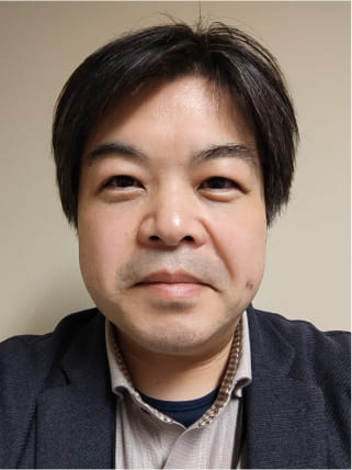
Specially Appointed Professor
Tomoyuki Suwa
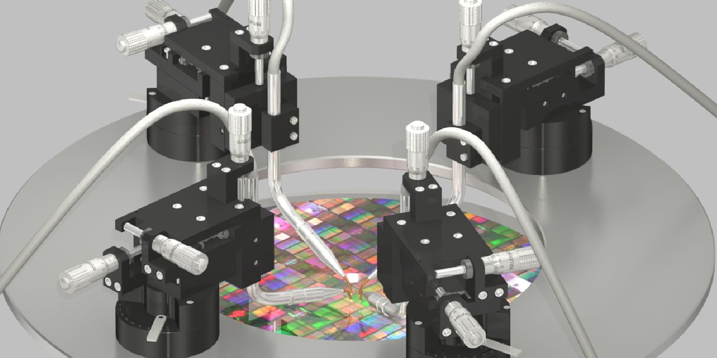
My research focuses primarily on the development of process technologies required for manufacturing high-performance semiconductors. In addition to developing surface control and thin-film deposition technologies capable of atomic-layer control for fine and complex geometries, I utilize X-ray-based measurement and analysis techniques to develop plasma equipment and process technologies for advanced micro-semiconductor manufacturing through industrial-academic collaboration.
BASE
-
Spintronics Low-Power Semiconductor Development Hub
Design, Prototype verification, Evaluation and System development for
・Power saving logic semiconductor,
・AI processor,
・Next generation embedded memory (MRAM) with spintronics technology.VIEW DETAIL
-
Hub for Semiconductor Manufacturing Process, Parts, Material and Image Sensors
R&D based on ultra-clean process technology and image sensor technology for
・Ultra-small particles during manufacturing,
・Visualize gas flows,
・Ultra-clean parts,
・High-performance image sensor, Wiring materialsVIEW DETAIL
-
MEMS Design/Process Development Demonstration Hub
R&D and technological evaluation/phototyping for advanced mounting technology for devices such as
・inertial sensor,
・photonics,
・Communication,
etc. for autonomous vehicles.VIEW DETAIL
-
Smart System Ultra-Integration Research and Development Center
This organization was reorganized and renamed in April 2026 to promote research into next-generation smart systems, including chiplet integration, 3D packaging, silicon photonics, quantum and biosensors, and the integration of edge AI.
VIEW DETAIL