Become the Semiconductor Talent
Shaping the Future.
World-Class Learning
at Tohoku University's
"S-Hub"
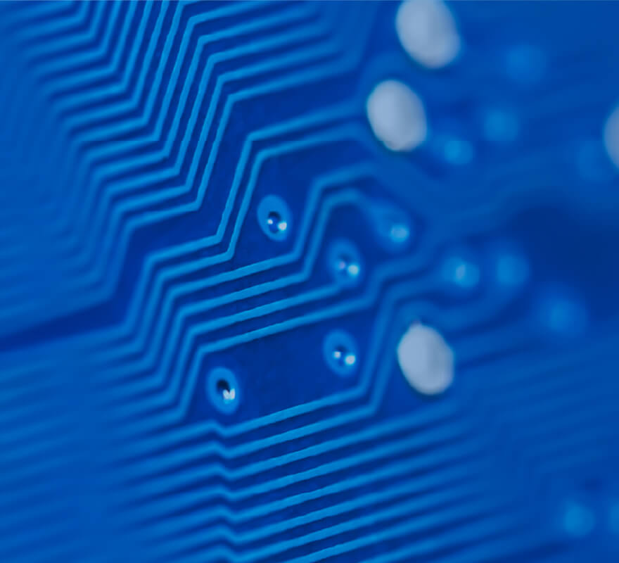
With the advancement of AI, the semiconductor industry is projected to reach a market scale of 150 trillion
yen by 2030. In response to the critical challenge of talent shortages, Tohoku University has established a
world-class educational hub where students can learn the entire process—from design and manufacturing to
materials—in an integrated manner.
Our programs are open not only to current students but also to students from other universities and working
professionals. Why not acquire the skills to lead the next generation of innovation?
A World-Class Educational Hub

-
1.Top-Level Environment
Leveraging over 150 semiconductor researchers and a massive cleanroom facility spanning a total area of 8,500m².
-
2.End-to-End Development System
Covering everything from semiconductor design and manufacturing to materials, equipment, inspection tools, and design support.
-
3.Open Learning
Targeting a wide range of individuals, from internal/external students to working professionals.
Target Profiles at S-Hub
Global Leaders
(Global Frontier Talent)
Individuals capable of solving social issues using design thinking and proposing innovative solutions.
Core Industry Personnel
(Industry Core Talent)
Individuals who strengthen the foundations of development and manufacturing through semiconductor design, production, quality control, and productivity improvement.
Five Practical Learning Contents
at S-Hub
- ・Semiconductor Educational Content Library
- ・e-Learning: Basic Semiconductor Course
- ・e-Learning: Advanced Semiconductor Course
- ・Tohoku University MOOC: "Introduction to Semiconductors" (Scheduled to open in FY2026)
- ・Semiconductor Hands-on Training
S-Hub continues to evolve. For more details on projects that will expand your future—including e-learning
registration,
the latest training information, and event updates—please visit the official website.