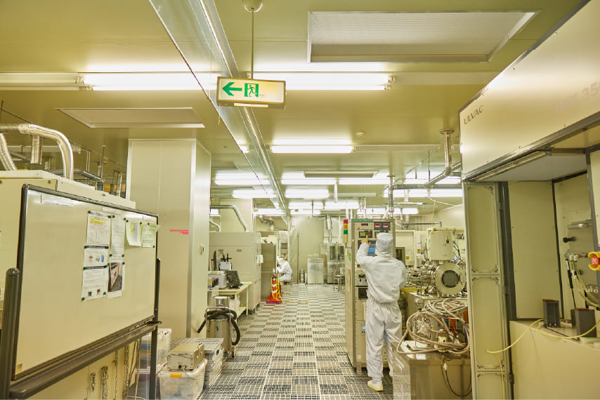
FACILITY

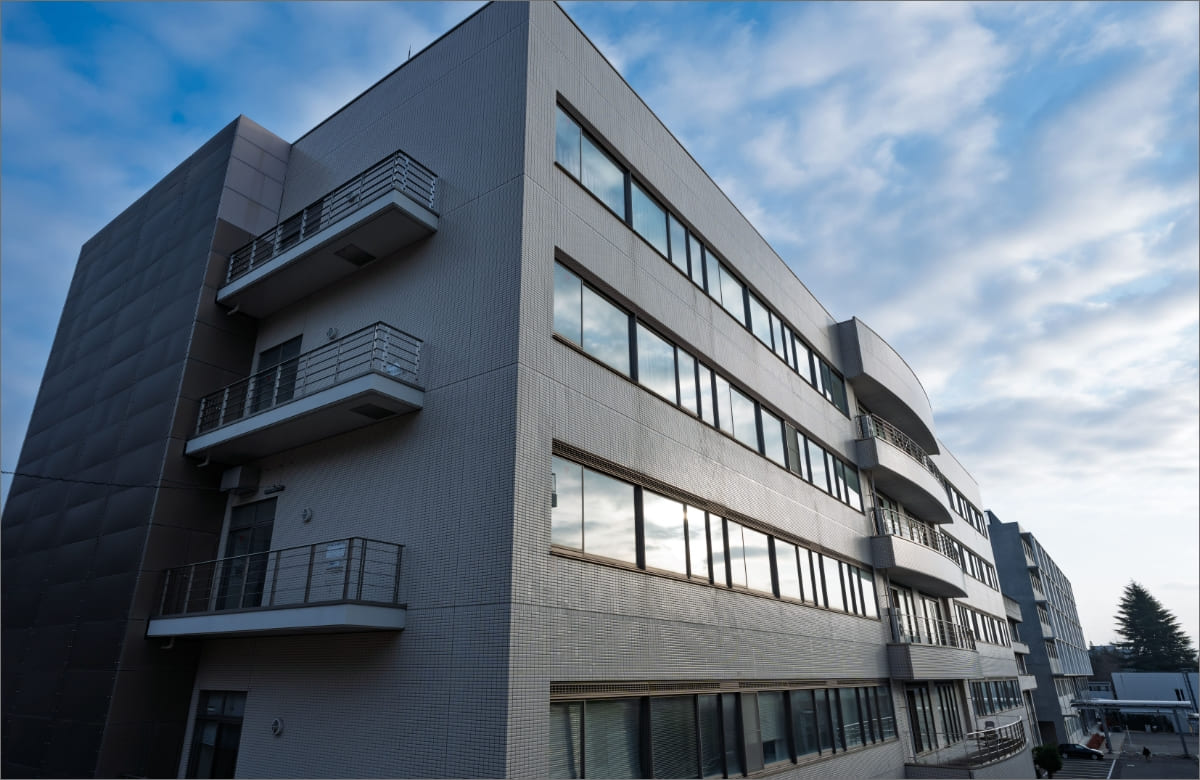
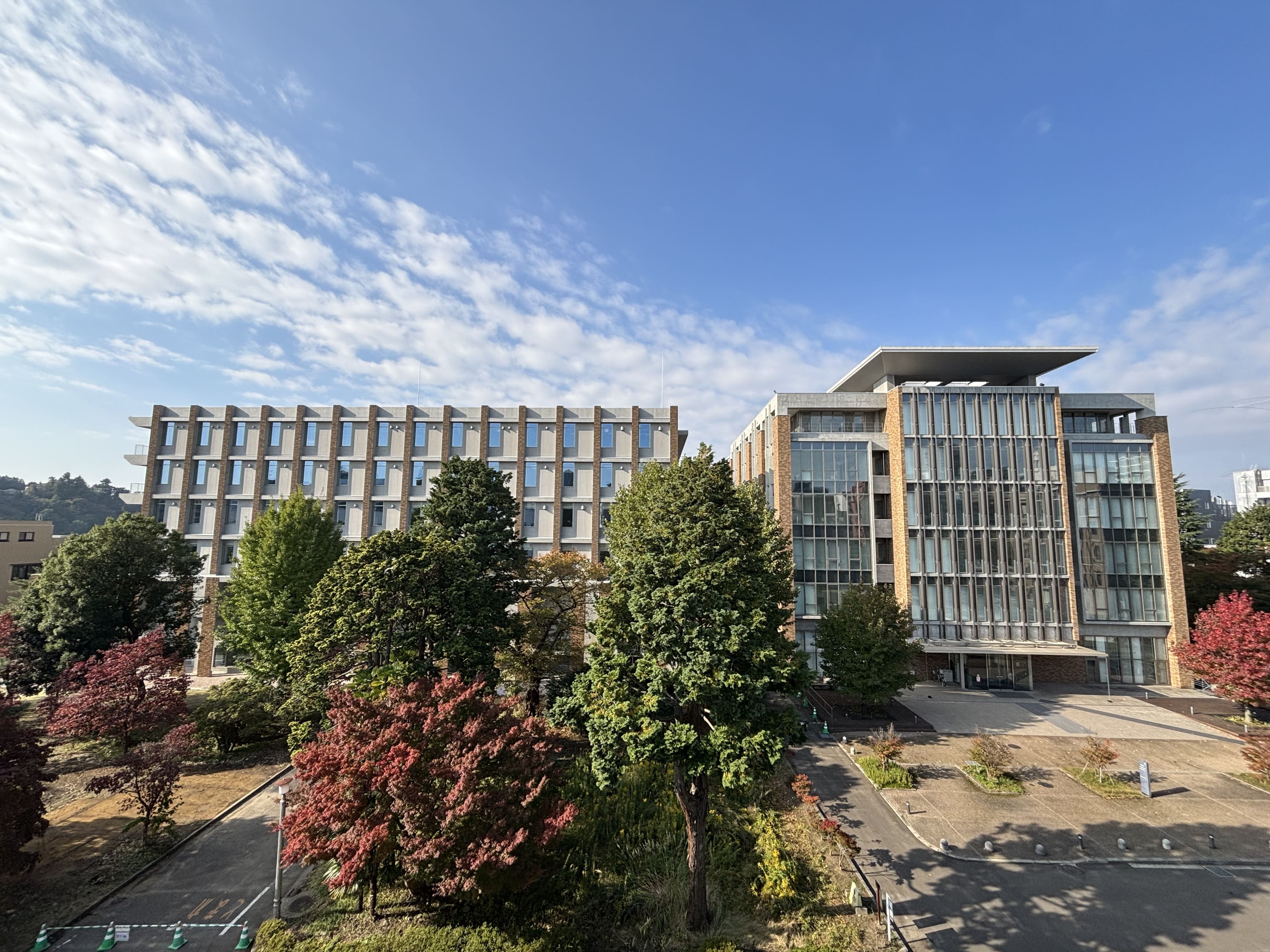
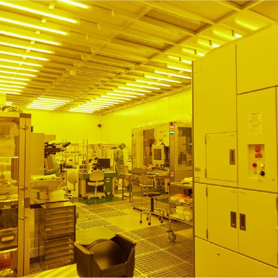
Center for Innovative Integrated Electronic Systems(CIES)
-
1,900㎡ CR & 300mm-Wafer line
-
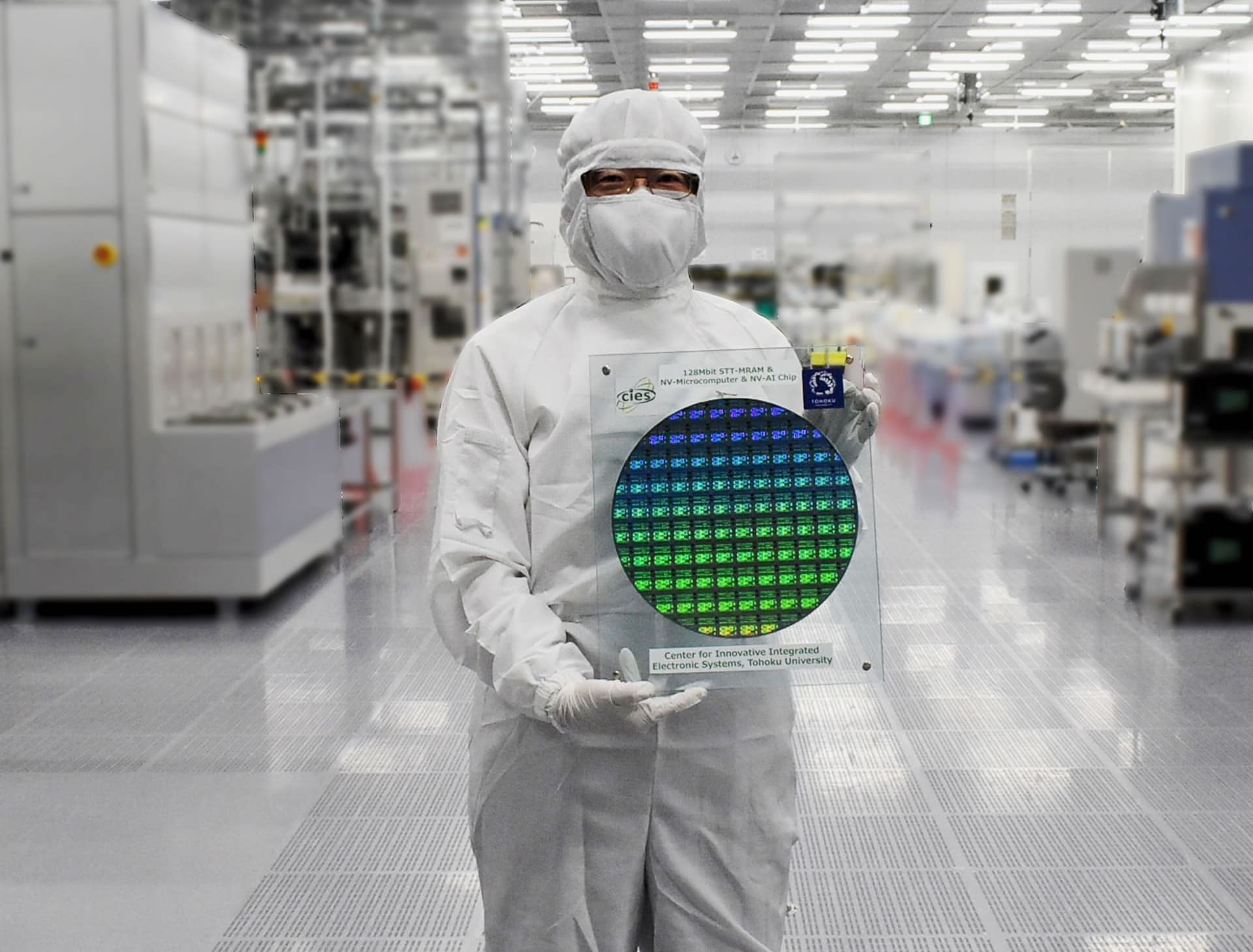
The world's only 300mm process-compatible prototyping line.
-
A comprehensive range of evaluation and analysis equipment for chip demonstration and testing
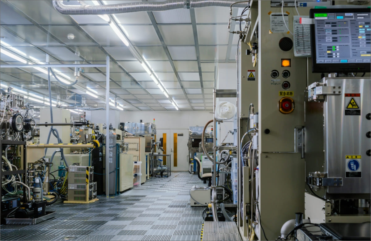
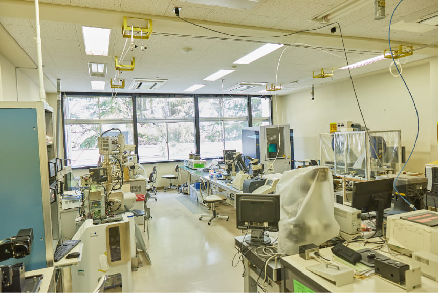
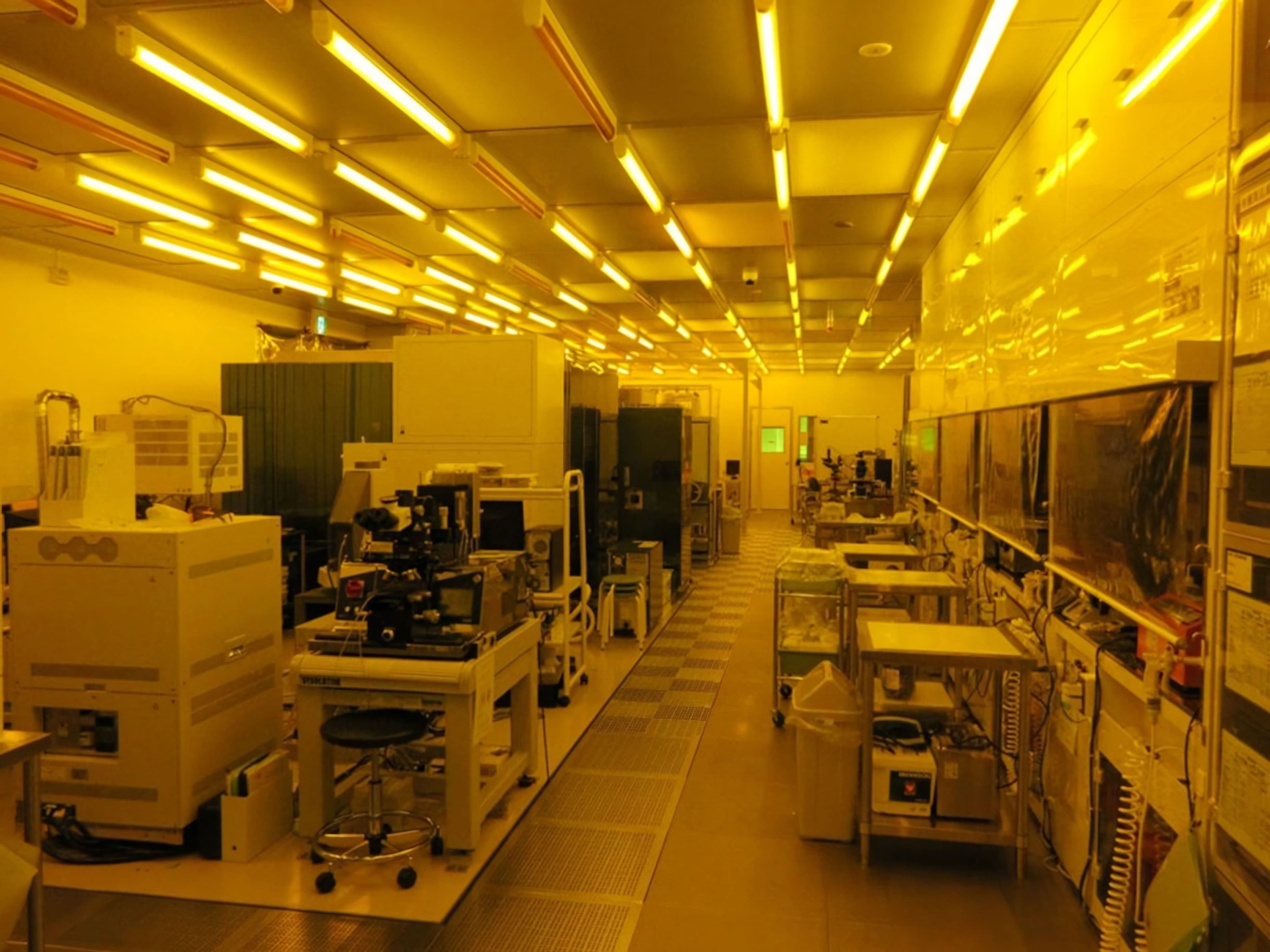
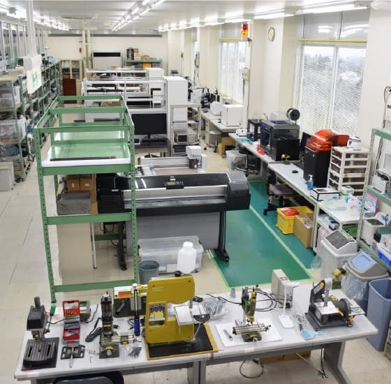
New Industry Creation Hatchery Center (NICHe)
-
Process floor : 739㎡/630㎡ (P2/ P1)
-
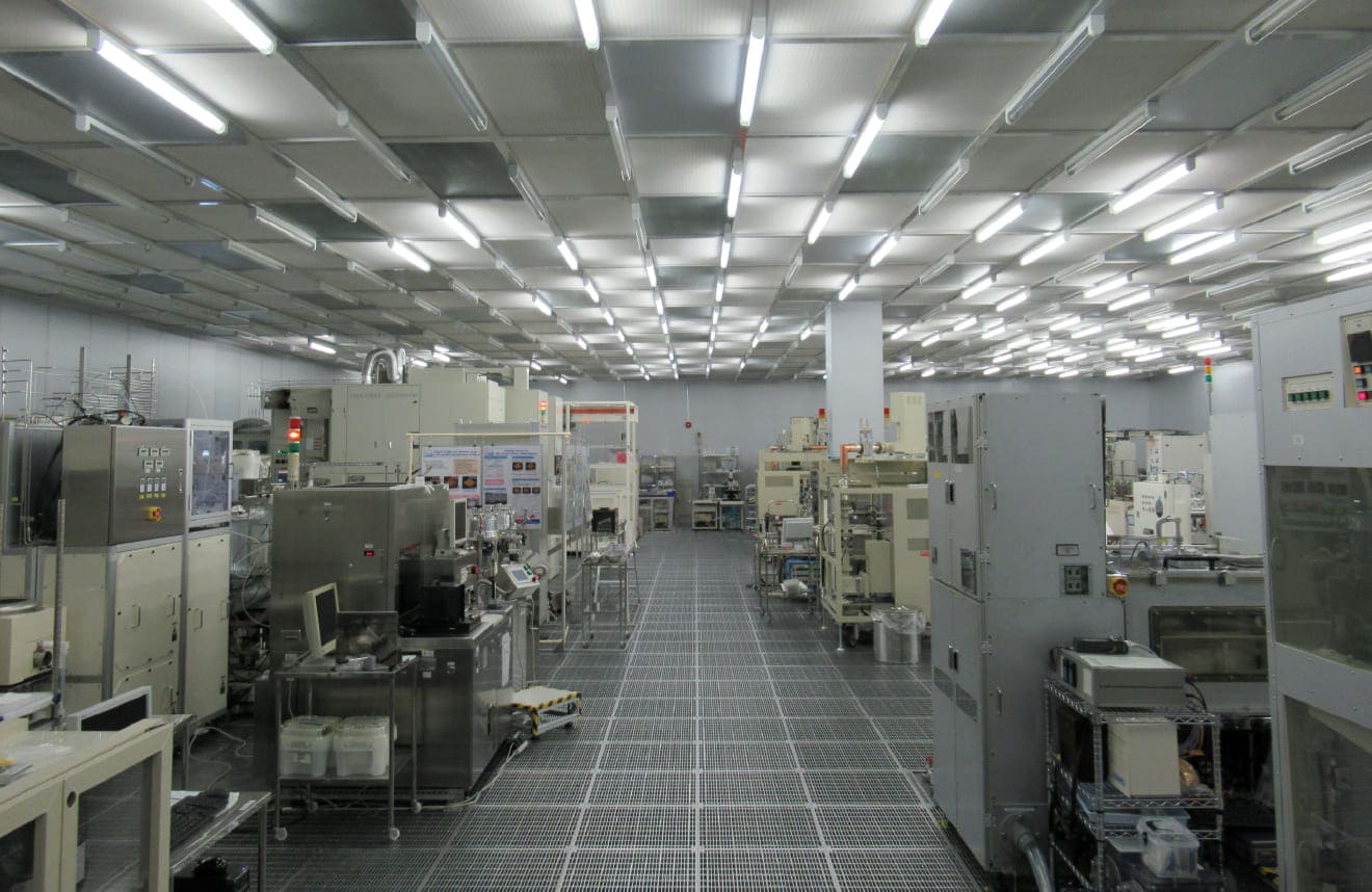
Experimental equipment in the cleanroom on the 4th floor of the Fluctuation-Free Facility for New Information Industry.
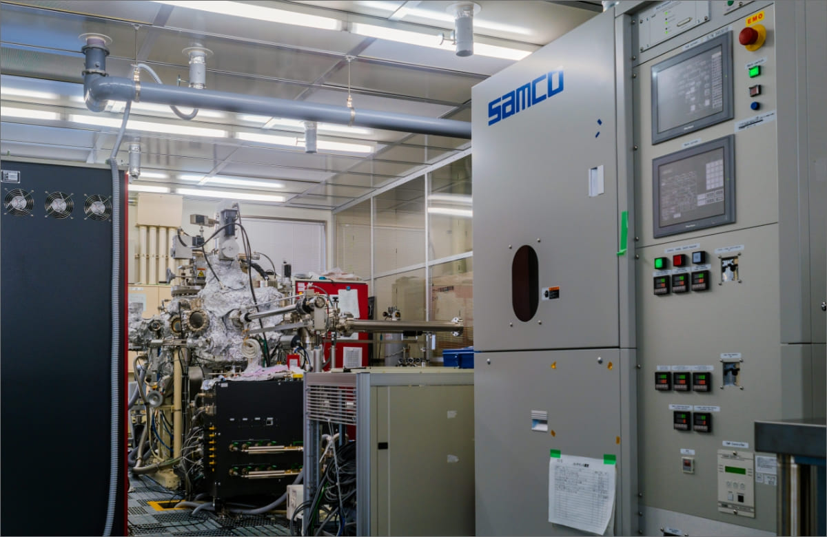
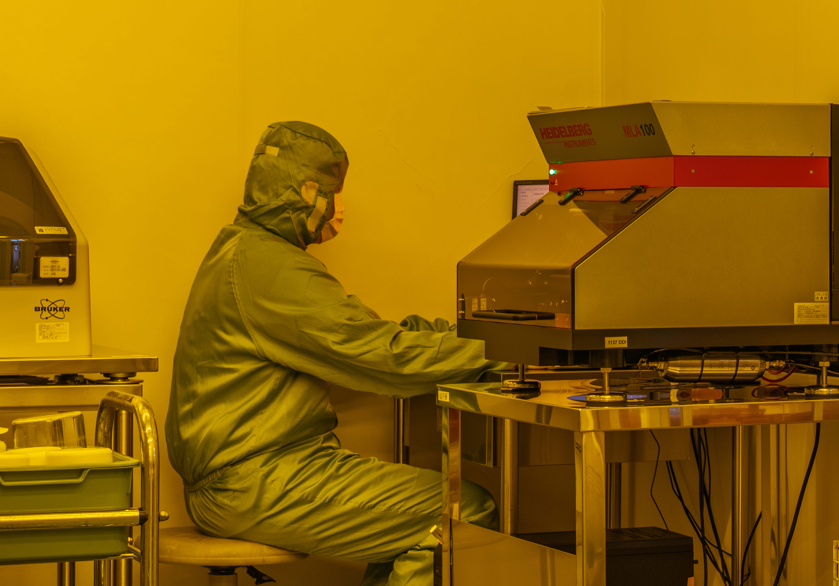
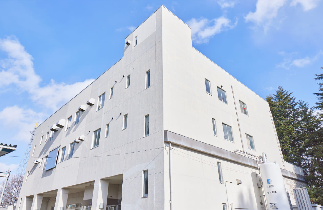
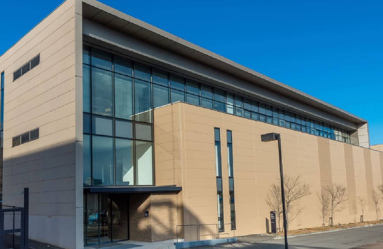
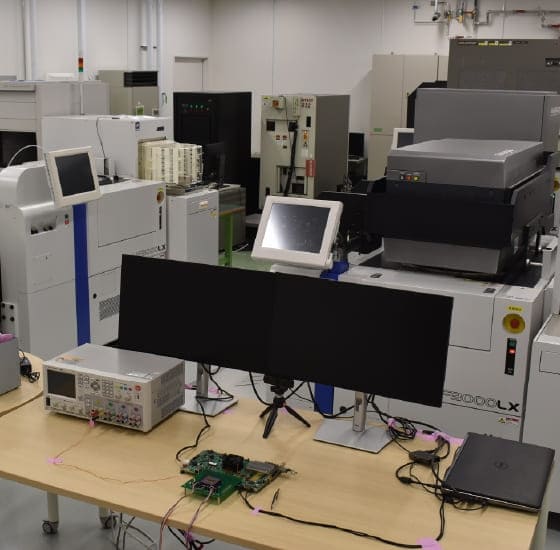
Micro System Integration Center (μSIC)
-
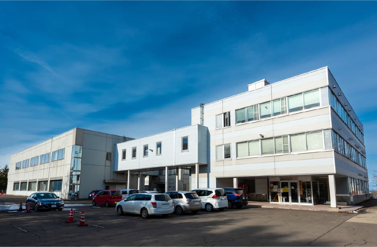
1,800㎡ Super CR, Prototype development with 4/6inch-wafer & Advanced Fusion Lab.(3F CR)
-
Utilizing the building that formerly housed the Semiconductor Research Institute—where Dr. Jun-ichi Nishizawa, known as "Mr. Semiconductor," served as Honorary Director—the facility boasts a 1,800㎡ cleanroom equipped with over 150 units of semiconductor manufacturing equipment, primarily for MEMS.
-
We also support electronic work and machining, providing an environment for the integrated prototyping, evaluation, and packaging of semiconductor devices. We actively support commercialization through collaboration with private enterprises.
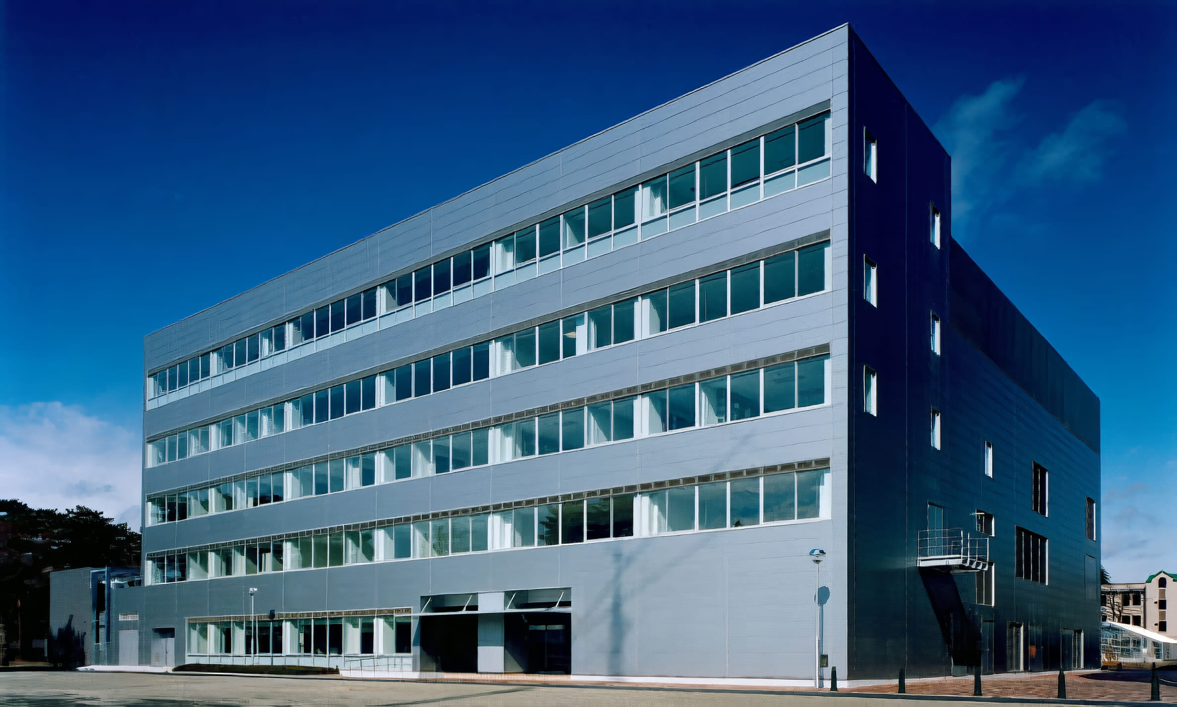
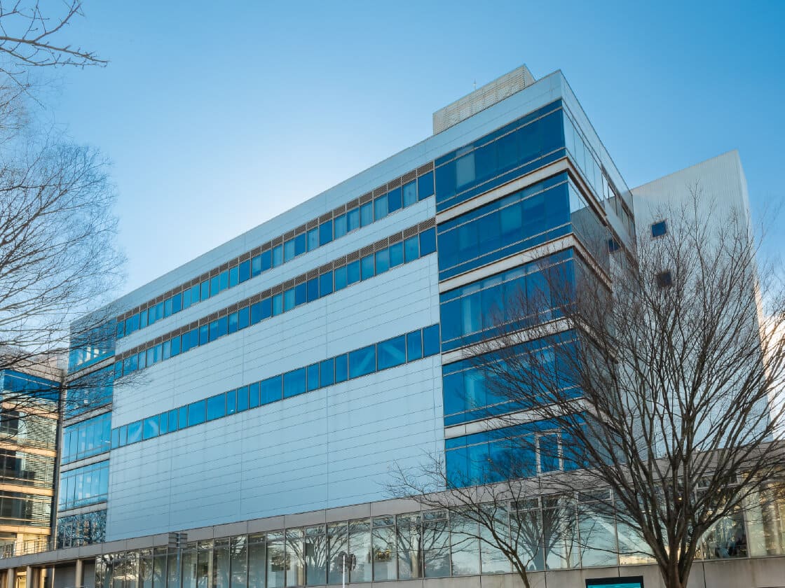
Material Innovation Center
-
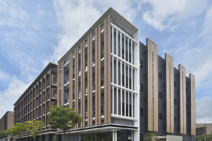
An open innovation hub in the field of materials science, housing university researchers and university-launched ventures (approx. 400㎡).
3GeV High-Brilliance Synchrotron Radiation Facility: NanoTerasu
-
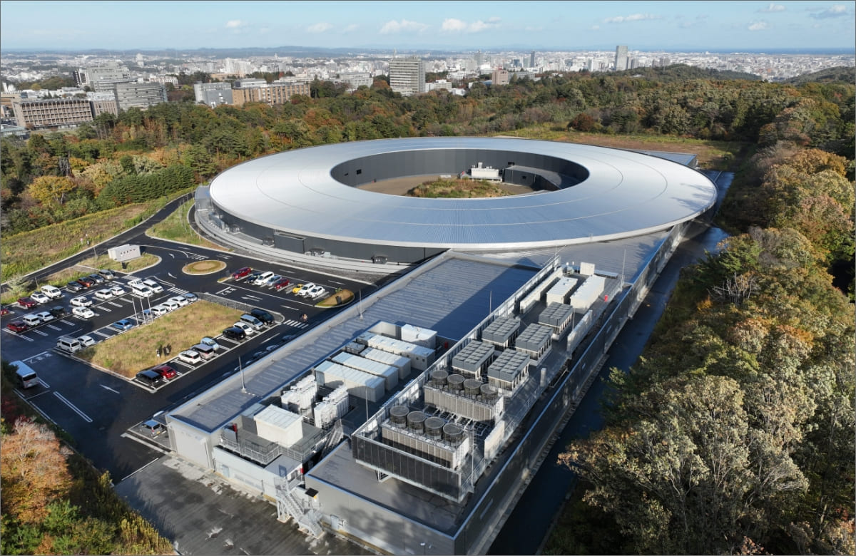
Operated through a public-private regional partnership.