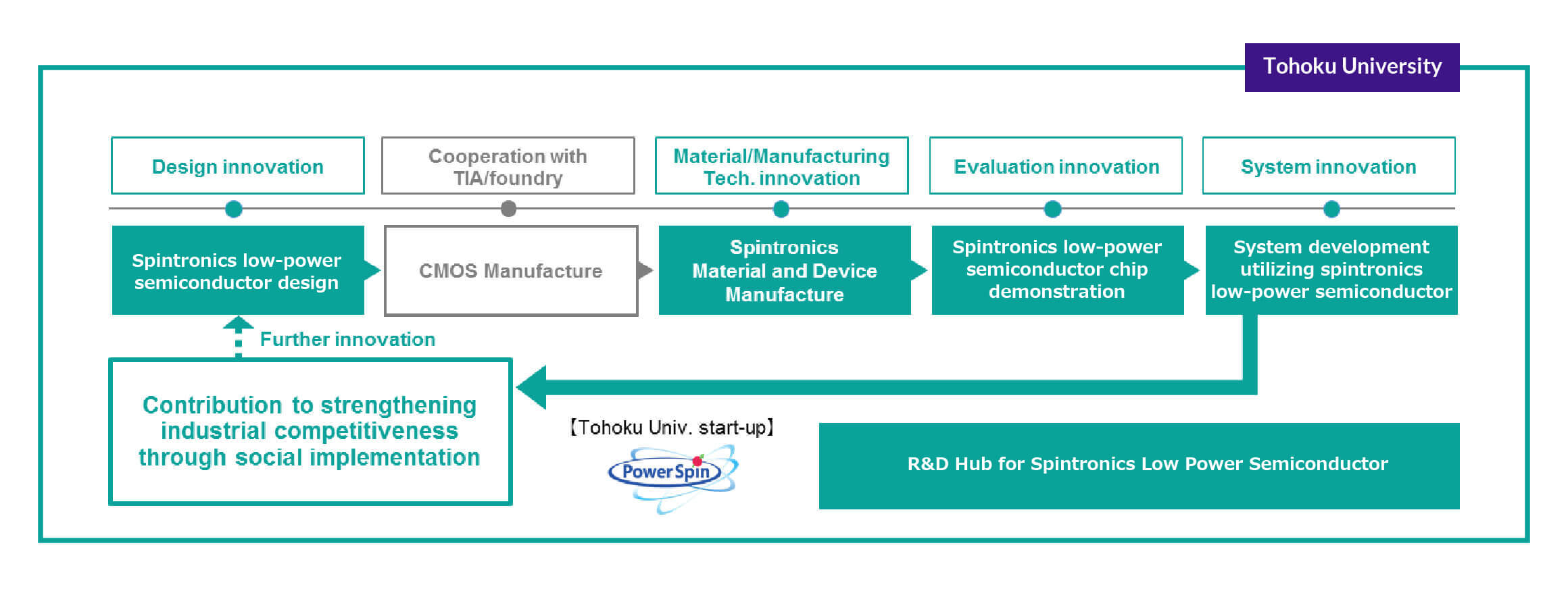
R&D Hub for Spintronics Low Power Semiconductor
This Hub has the world‘s only 300mm-wafer compatible R&D facility in spintronics semiconductor development.
At this hub, we can consistently develop from design, prototyping, evaluation, systematization / Creation of world-leading power-saving technology.
As a result, we will lead the world in the development of spintronics logic semiconductors with 1/100 power consumption, which is a world-leading power-saving technology, and its application systems.